
AJW PCB
HDI · Multilayer · LED · Rigid-Flex · Shenzhen, China

High-Precision PCB Manufacturer for Electronics Teams

Shenzhen AJW Electronics Co., Ltd. manufactures high-precision multilayer, HDI, LED and rigid-flex PCBs — fast prototypes and small-to-medium batches.

15,000–20,000+ m²/month, RMB 16–20M output, from design to delivery.

2016Founded
5,000 m²Shenzhen plant
15–20k m²Monthly output
64Max layers
Manufacturing services

End-to-end PCB solutions

A technology-led specialist in high-end PCBs — from design review to delivery, custom solutions for every project.

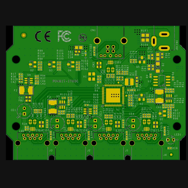
3D render of a high-multilayer PCB board
01 · PCB

PCB fabrication

High-multilayer, HDI, LED and rigid-flex boards. Blind/buried vias, heavy copper and high-frequency materials supported.

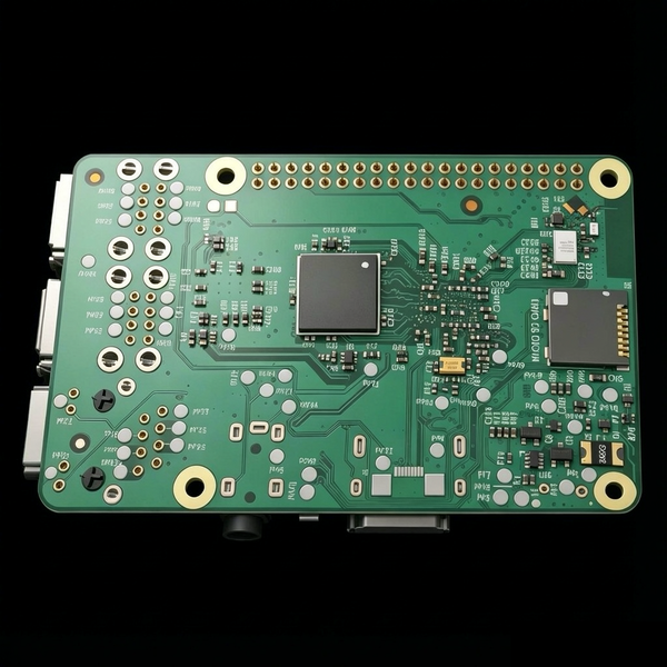
3D render of an assembled PCBA board
02 · PCBA

PCBA assembly

Assembly coordinated around your PCB design, bill of materials and assembly documentation.

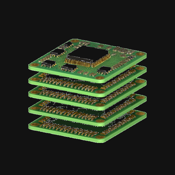
3D render of PCB boards representing fast turnaround
03 · Fast turnaround

Prototype to batch

48-hour multilayer and 96-hour HDI turnaround, 20-minute quotation and real-time order tracking.

Product display

See what we build

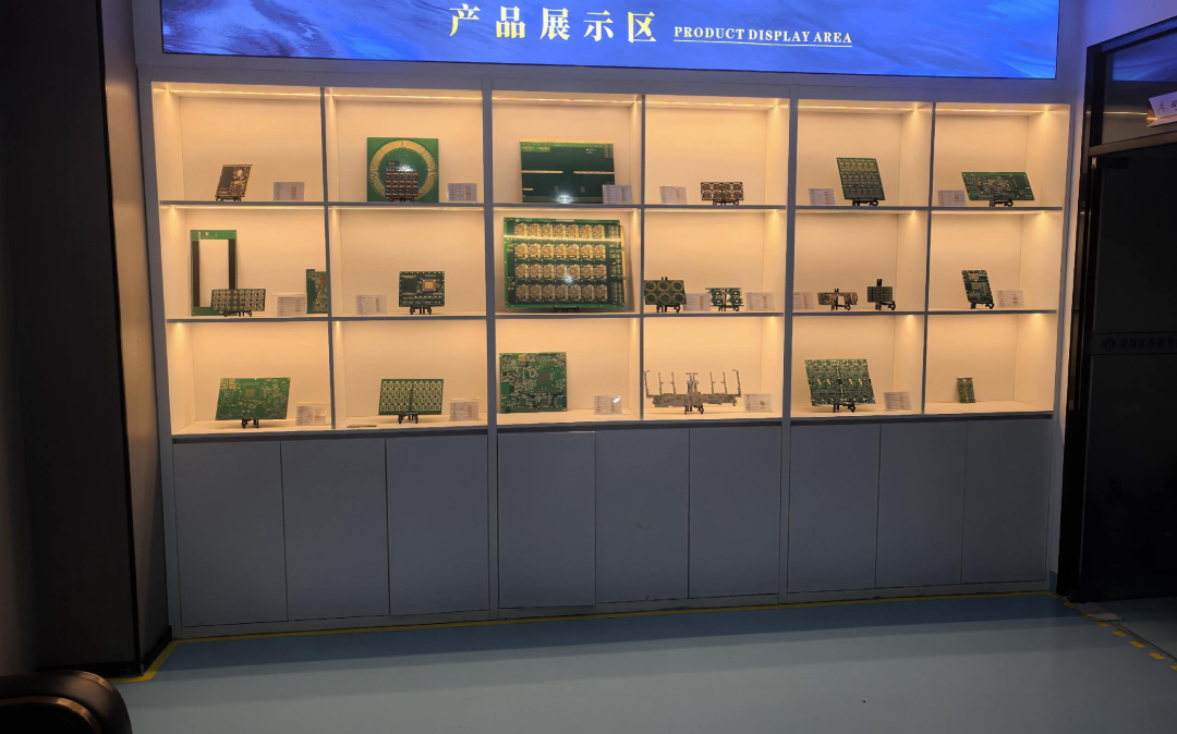
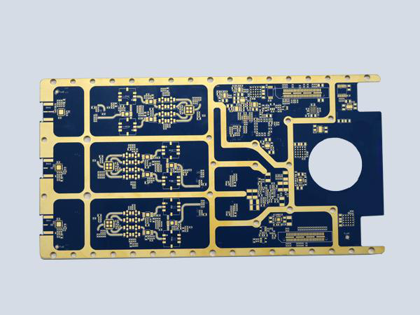
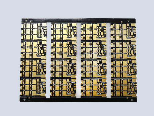
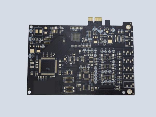
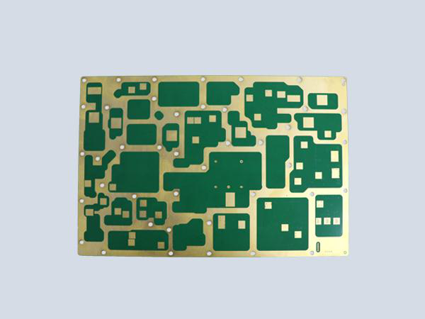
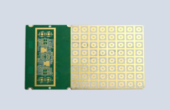
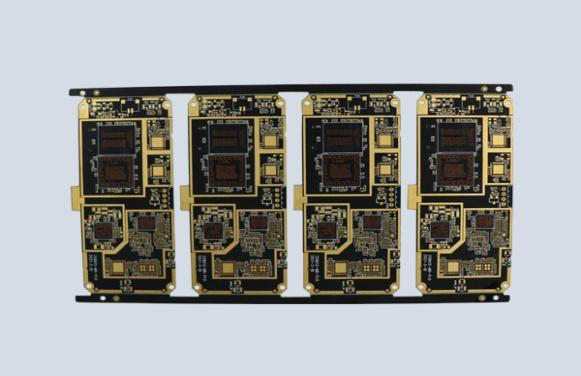
Samples from our product display area — multilayer, HDI, heavy-copper, gold-finger, rigid-flex and high-frequency boards.

Capability

Manufacturing capability overview

High-layer-count, high-precision, high-complexity PCB production since 2016. These stated limits are a reference — confirm each design with engineering before ordering.

Item High Multilayer Blind/Buried Via Heavy-Copper HF / High-Speed Rigid-Flex
MaterialFR-4FR-4FR-4RO / TU / F4BFR-4 + PI
Max. layers6432203024
Board thickness0.3–7.0 mm0.4–5.0 mm0.4–7.0 mm0.4–7.0 mm0.4–7.0 mm
Copper thickness0.5–2 oz1/3–2 oz3–10 oz0.5–4 oz1/3–2 oz
Min. hole size0.1 mmLaser via 0.05 mm0.1 mm0.1 mm0.1 mm
Line / space2/2 mil2/2 mil—2/2 mil2/2 mil
Aspect ratio≤ 15:1≤ 15:1≤ 15:1≤ 15:1≤ 10:1
Max. size550 × 800 mm400 × 800 mm550 × 800 mm550 × 800 mm300 × 800 mm

Surface finish: OSP, ENIG, immersion tin, immersion silver, ENEPIG, HASL, electroplated gold.

Materials

Materials and special processes

Qualified materials from leading suppliers, plus a full range of special processes for demanding designs.

Laminate

Base materials

Shengyi, ITEQ, Kingboard (KB), Mingguang Ruizhi, Rogers, Panasonic, TUC, Isola.

Finish & ink

Surface & solder mask

ENIG, immersion tin, immersion silver, lead-free HASL, ENIG + OSP, electroplated gold. Solder mask ink: Taiyo, Guangxin.

Special processes

Advanced capabilities

Castellated holes, metal edging, impedance control, gold fingers, asymmetric copper, heavy copper, step board. Prepreg: Shengyi, USC. EMI film: Sanhui, Toyo. Conductive adhesive: TATSUTA. Double-sided tape: 3M, Tesa.

Equipment

Production equipment

In-house equipment for every stage — drilling, plating, imaging, lamination, testing and routing.

PCB LDI imaging equipment

LDI Imaging

Laser direct imaging for fine line and space patterns.

PCB lamination press

Lamination

Lamination for multilayer stack-up and build.

PCB flying probe tester

Flying Probe

Flying probe electrical test for prototypes and small batches.

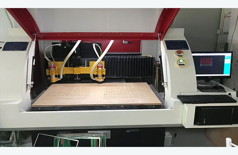
PCB CNC routing machine

CNC Routing

CNC routing for board profiling and depaneling.

PCB CNC drilling machine

CNC Drill

CNC drilling for precision through-holes and vias.

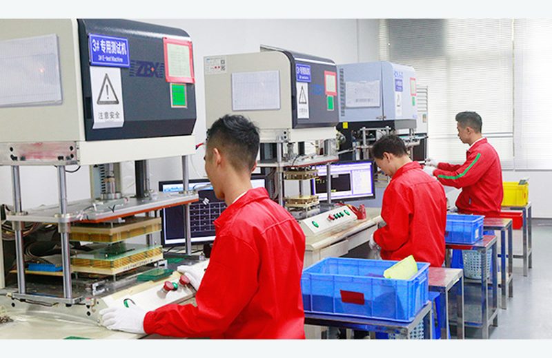
PCB fixture test equipment

Fixture Test

Fixture test for electrical verification of production boards.

Advantages

Why teams choose AJW PCB

48hMultilayer turnaround

Fast multilayer prototypes delivered within 48 hours.

96hHDI turnaround

HDI boards with blind vias to 40 layers in 96 hours.

20minQuotation

Real-time order tracking and 20-minute quotations.

10+Years experience

Engineers with 10+ years experience in high-end PCBs.

40LHDI / blind vias

HDI and blind/buried via capability up to 40 layers.

16–20MMonthly output (RMB)

15,000–20,000+ m² monthly production capacity.

Customer order process

From files to delivery

01

Requirements review

Project feasibility and requirements review.

02

Send Gerber & BOM

Gerber & BOM to sales@ajwpcb.com.cn. State process, quantity and contact details.

03

Confirm & produce

We confirm process and plan, then start production.

04

Payment & delivery

Payment settled; production and delivery on time.

Common questions

PCB and PCBA questions

What files should I send for a quote?

For PCB fabrication, send Gerber files. For PCBA, include the BOM. Also state process, quantity, surface finish, target timing and application.

What are your lead times?

Multilayer prototypes within 48 hours, HDI boards within 96 hours. Batch lead times depend on the design and quantity.

Which materials and finishes do you support?

FR-4, high-frequency materials (Rogers, TUC, etc.) and rigid-flex. Finishes include ENIG, immersion tin/silver, HASL, ENEPIG and electroplated gold.

Can every design meet the listed maximum capability?

Not automatically. The capability figures are references; engineering confirms feasibility for the specific stack-up and design.

Inside the factory

Watch AJW PCB at work

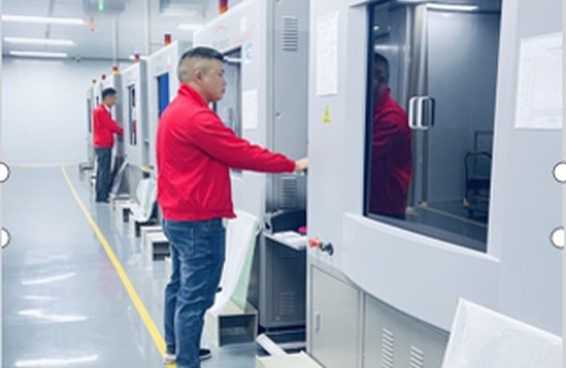
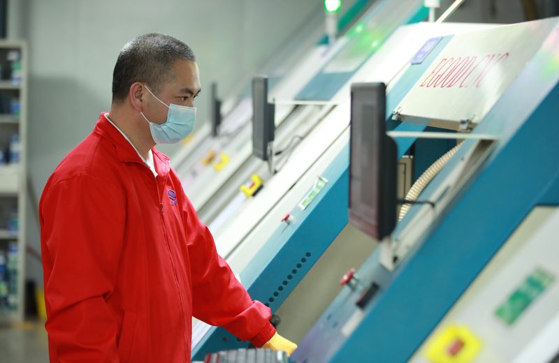
A look inside our Shenzhen plant — from drilling and imaging to final inspection of high-precision boards.

Factory tourHigh-precision PCB production at our Shenzhen plant

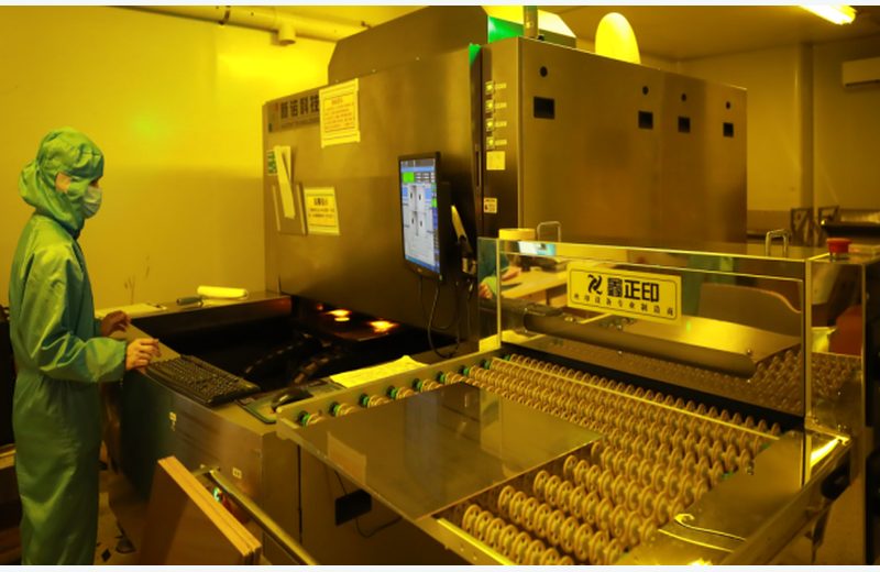
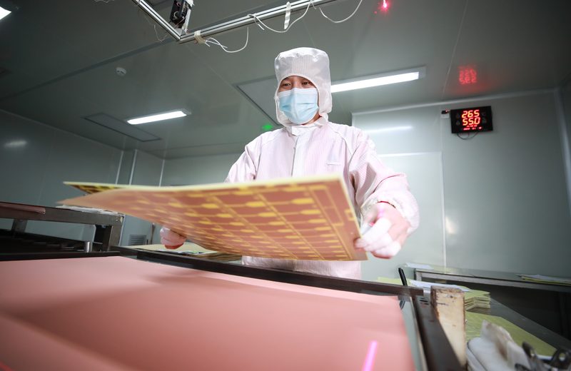
A walk through our Shenzhen plant — from CNC drilling and laser imaging to lamination, AOI and final electrical test.

Take a virtual walk through our 5,000 m² Shenzhen facility. The tour follows a board from blank laminate through CNC drilling, laser direct imaging and plating, then into lamination, solder mask and surface finish. Every panel then passes automated optical inspection (AOI) and 100% electrical test before routing and final packing. It is the same repeatable process we run for prototypes and production alike, backed by 10+ years of engineering experience in high-end PCBs.

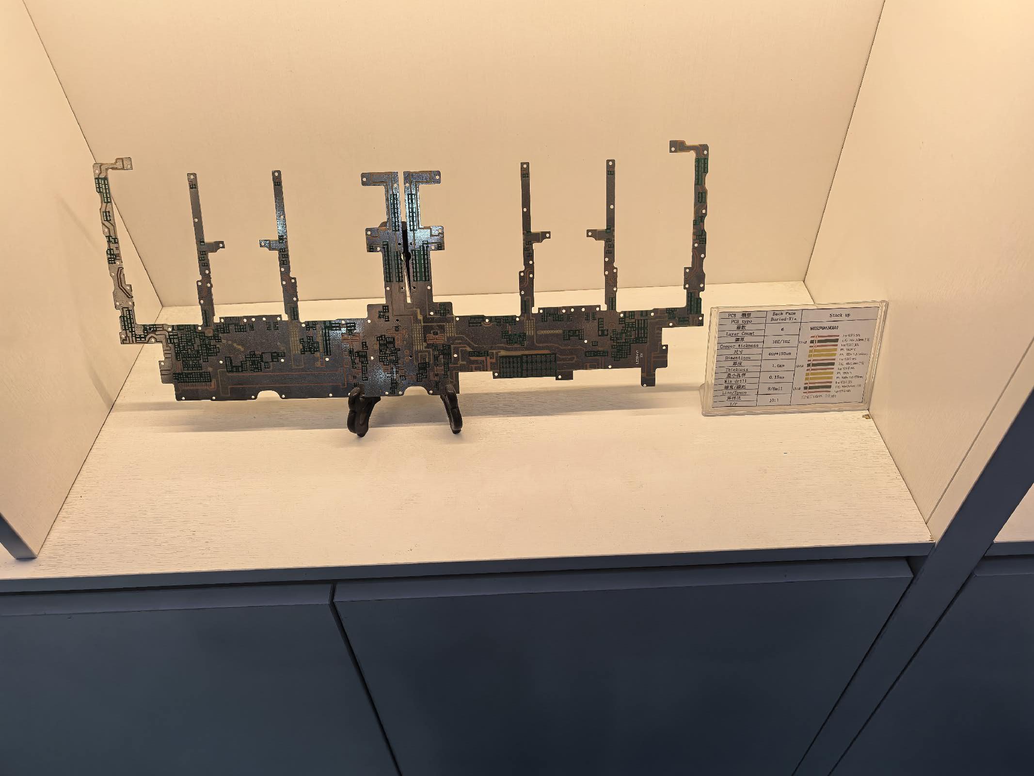
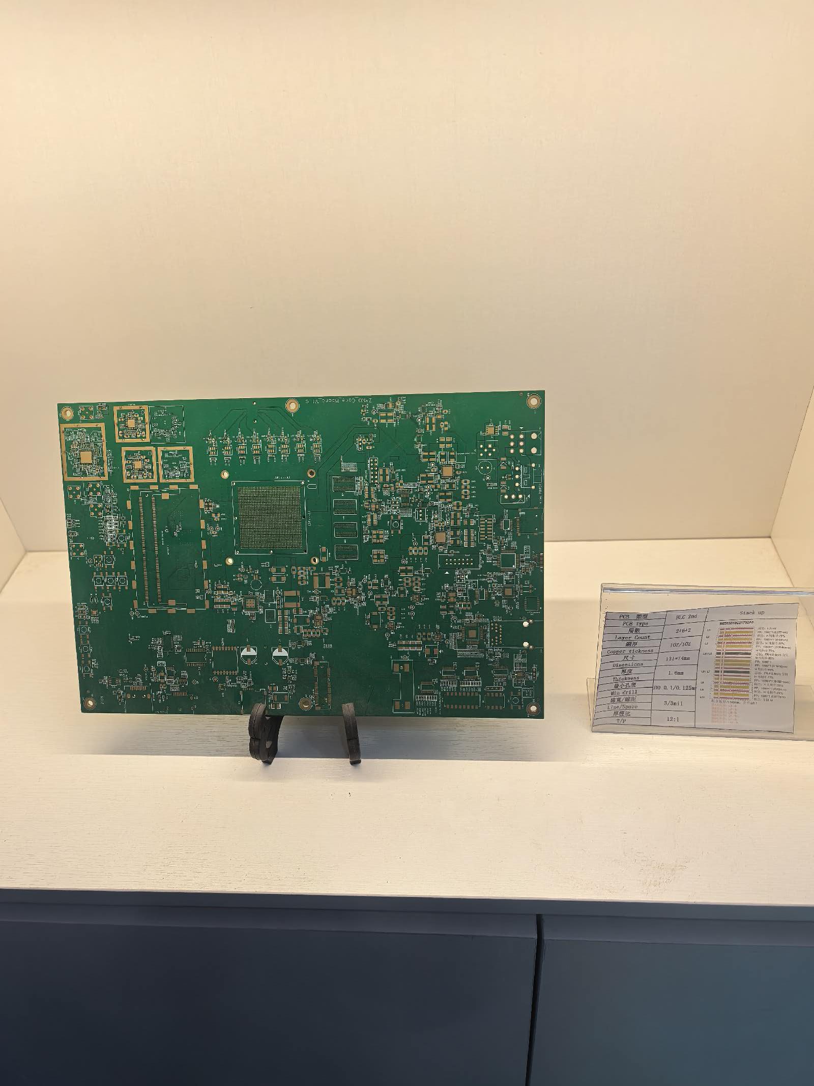
AJW PCB product display shelves
Product displayBoard samples on our showroom shelves

Board samples on our showroom shelves.

Our showroom shelves hold working samples of the boards we manufacture daily — high-multilayer, HDI, heavy-copper, gold-finger, castellated and high-frequency designs. Seeing a finished board up close is often the fastest way to judge surface finish, hole quality and registration. If you would like a sample pack for your next project, contact sales@ajwpcb.com.cn and we will arrange it.

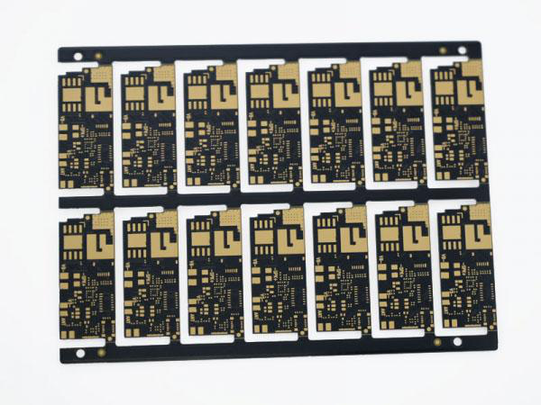
Finished AJW PCB panel
Finished boardsMultilayer panels ready for delivery

Multilayer panels ready for delivery.

After routing, each panel is cleaned, edge-inspected and vacuum-packed before it leaves the plant. Finished boards are delivered in standard anti-static packaging with full documentation, so they arrive ready for your assembly line. We support small-to-medium batches as well as fast-turn prototypes, with real-time order tracking from lamination to dispatch.

Every board passes through automated optical and electrical inspection before it leaves our Shenzhen plant, so you receive the same repeatable quality on prototypes and production runs alike.
Insights & resources

PCB knowledge and news

Practical guidance from our engineering team — material selection, design rules and industry updates for electronics teams.

Multilayer PCB stack-up
Guide · Feb 2026

How to choose the right PCB laminate

FR-4, high-frequency and high-Tg materials explained — and how to pick the right one for your design, cost and reliability targets.

The laminate is the foundation of every PCB — it determines electrical performance, thermal stability and cost. Standard FR-4 suits most digital boards below 1 GHz and is the most economical choice. For RF, radar and 5G designs, choose low-loss high-frequency materials such as Rogers or Panasonic M6, which keep signal attenuation low at high frequencies. For automotive, industrial or power electronics that run hot, a high-Tg laminate (Tg 170 °C or above) resists delamination through repeated thermal cycling. When in doubt, send us your stack-up and operating conditions — our engineers will recommend a material that balances performance, reliability and budget.

Read more →
HDI heavy copper PCB
Guide · Jan 2026

HDI vs. multilayer: which do you need?

A plain-language comparison of HDI and standard multilayer boards — blind/buried vias, density and when each makes sense.

Standard multilayer boards use through-hole vias that pass all the way through the stack, which consumes routing space on every layer. HDI (high-density interconnect) replaces them with blind and buried vias, laser-drilled microvias and fine line/space down to 50 µm, so more circuitry fits in a smaller area. Choose HDI when your design is space-constrained — wearables, smartphones, high-pin-count BGAs — or when signal integrity demands short, controlled paths. Choose conventional multilayer when cost is the priority and density is moderate. AJW supports both, up to 64 layers for high-multilayer and HDI to 40 layers.

Read more →
Gold finger edge connector PCB
News · 2026

Company update: expanding quick-turn capacity

Our latest production updates and how we keep 48-hour multilayer and 96-hour HDI turnarounds reliable at scale.

AJW has expanded its Shenzhen quick-turn line to keep 48-hour multilayer and 96-hour HDI turnarounds reliable even as volume grows. The expansion adds in-house drilling, laser imaging and automated optical inspection capacity, so prototypes ship without waiting on outside vendors. For engineering teams, this means faster iteration cycles: upload Gerber and BOM, get a 20-minute quotation, and track your order in real time from lamination to final electrical test. Contact sales@ajwpcb.com.cn to discuss your next fast-turn project.

Read more →
Company information

About Shenzhen AJW Electronics Co., Ltd.

Founded in 2016 with RMB 5M capital and RMB 80M in fixed assets, AJW Electronics operates a 5,000 m² plant in Shenzhen. We manufacture high-precision multilayer, HDI, LED and rigid-flex PCBs — fast prototypes and small-to-medium batches — with end-to-end custom solutions from design to delivery.

AddressDawangshan 2nd Industrial Zone, Shajing, Shenzhen
Emailsales@ajwpcb.com.cn
WhatsApp+86 15013696852